- 您现在的位置:买卖IC网 > Sheet目录3876 > PIC16F639-E/SS (Microchip Technology)IC MCU FLASH 2KX14 20SSOP
Micrel, Inc.
KSZ8841-PMQL
October 2007
9
M9999-100407-1.5
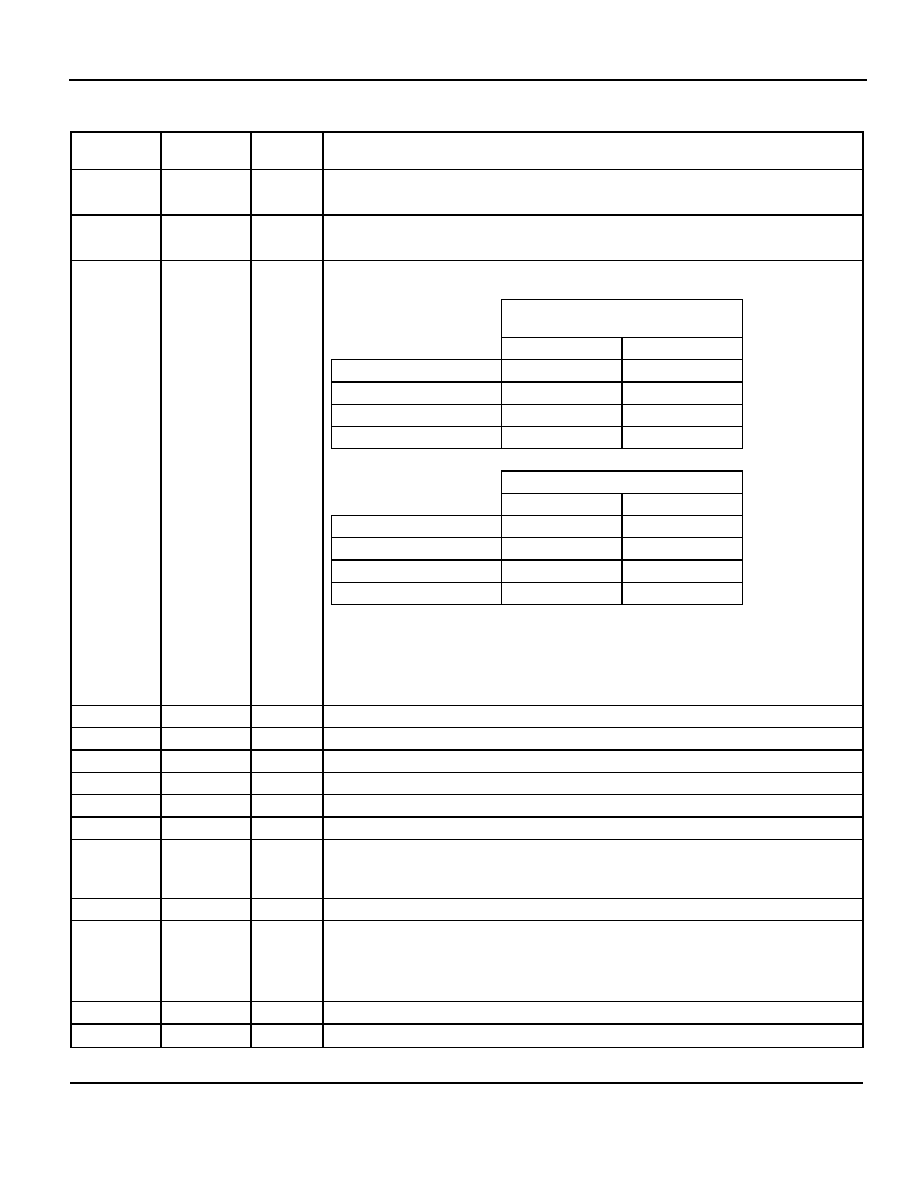
Pin Description
Pin
Number
Pin
Name
Type
Pin Function
1
TEST_EN
I
Test Enable
For normal operation, pull-down this pin to ground.
2
SCAN_EN
I
Scan Test Scan Mux Enable
For normal operation, pull-down this pin to ground.
3
4
5
P1LED2
P1LED1
P1LED0
Opu
Port 1 LED indicators
1 defined as follows:
LEDs turn on when low.
Chip Global Control Register:
CGCR bit [15,9]
[0,0] Default
[0,1]
P1LED3
2
—
P1LED2
Link/Act
100Link/Act
P1LED1
Full duplex/Col
10Link/Act
P1LED0
Speed
Full duplex
Reg. CGCR bit [15,9]
[1,0]
[1,1]
P1LED3
2
Act
—
P1LED2
Link
—
P1LED1
Full duplex/Col
—
P1LED0
Speed
—
Notes
:
1. Link = On; Activity = Blink; Link/Act = On/Blink; Full Dup/Col = On/Blink;
Full Duplex = On (Full duplex); Off (Half duplex)
Speed = On (100BASE-T); Off (10BASE-T)
2. P1LED3 is pin 27.
6
NC
—
No connect
7
NC
—
No connect
8
NC
—
No connect
9
DGND
Gnd
Digital ground
10
VDDIO
P
3.3V digital I/O VDD
11
NC
—
No connect
12
PCLK
Ipd
PCI Bus Clock
This Clock provides the timing for all PCI bus phases. The rising edge defines the start
of each phase. The clock maximum frequency is 33MHz.
13
NC
—
No connect
14
PMEN
Opu
Power Management Enable
Asserted low.
When asserted, this signal indicates that a Wake-on-LAN packet has been received in
this Ethernet MAC chip.
15
NC
—
No connect
16
INTRN
Opd
Interrupt Request
发布紧急采购,3分钟左右您将得到回复。
相关PDF资料
PIC18LF24K22-I/SS
IC PIC MCU 16KB FLASH 28SSOP
PIC24F08KL402-I/ML
IC MCU 16BIT 8KB FLASH 28-QFN
PIC24F08KL302-I/SP
IC MCU 16BIT 8KB FLASH 28-SPDIP
PIC16LF1938-I/ML
IC MCU 8BIT FLASH 28QFN
PIC24F08KL402-I/MQ
IC MCU 16BIT 8KB FLASH 28-QFN
PIC16LF1938-I/MV
IC MCU 8BIT 28KB FLASH 28UQFN
PIC18F24K22-I/SS
IC PIC MCU 16KB FLASH 28SSOP
PIC16F1938-I/ML
IC MCU 8BIT FLASH 28QFN
相关代理商/技术参数
PIC16F639-I/P
功能描述:8位微控制器 -MCU 4kb 128 RAM 12 I/O RoHS:否 制造商:Silicon Labs 核心:8051 处理器系列:C8051F39x 数据总线宽度:8 bit 最大时钟频率:50 MHz 程序存储器大小:16 KB 数据 RAM 大小:1 KB 片上 ADC:Yes 工作电源电压:1.8 V to 3.6 V 工作温度范围:- 40 C to + 105 C 封装 / 箱体:QFN-20 安装风格:SMD/SMT
PIC16F639-I/SO
功能描述:8位微控制器 -MCU 4kb 128 RAM 12 I/O RoHS:否 制造商:Silicon Labs 核心:8051 处理器系列:C8051F39x 数据总线宽度:8 bit 最大时钟频率:50 MHz 程序存储器大小:16 KB 数据 RAM 大小:1 KB 片上 ADC:Yes 工作电源电压:1.8 V to 3.6 V 工作温度范围:- 40 C to + 105 C 封装 / 箱体:QFN-20 安装风格:SMD/SMT
PIC16F639-I/SS
功能描述:8位微控制器 -MCU 4kb 128 RAM 12 I/O RoHS:否 制造商:Silicon Labs 核心:8051 处理器系列:C8051F39x 数据总线宽度:8 bit 最大时钟频率:50 MHz 程序存储器大小:16 KB 数据 RAM 大小:1 KB 片上 ADC:Yes 工作电源电压:1.8 V to 3.6 V 工作温度范围:- 40 C to + 105 C 封装 / 箱体:QFN-20 安装风格:SMD/SMT
PIC16F639-I/SS
制造商:Microchip Technology Inc 功能描述:8-Bit Microcontroller IC
PIC16F639T-I/SO
功能描述:8位微控制器 -MCU 4kb 128 RAM 12 I/O RoHS:否 制造商:Silicon Labs 核心:8051 处理器系列:C8051F39x 数据总线宽度:8 bit 最大时钟频率:50 MHz 程序存储器大小:16 KB 数据 RAM 大小:1 KB 片上 ADC:Yes 工作电源电压:1.8 V to 3.6 V 工作温度范围:- 40 C to + 105 C 封装 / 箱体:QFN-20 安装风格:SMD/SMT
PIC16F639T-I/SS
功能描述:8位微控制器 -MCU 4kb 128 RAM 12 I/O RoHS:否 制造商:Silicon Labs 核心:8051 处理器系列:C8051F39x 数据总线宽度:8 bit 最大时钟频率:50 MHz 程序存储器大小:16 KB 数据 RAM 大小:1 KB 片上 ADC:Yes 工作电源电压:1.8 V to 3.6 V 工作温度范围:- 40 C to + 105 C 封装 / 箱体:QFN-20 安装风格:SMD/SMT
PIC16F648A-E/ML
功能描述:8位微控制器 -MCU 7KB 256 RAM 16 I/O RoHS:否 制造商:Silicon Labs 核心:8051 处理器系列:C8051F39x 数据总线宽度:8 bit 最大时钟频率:50 MHz 程序存储器大小:16 KB 数据 RAM 大小:1 KB 片上 ADC:Yes 工作电源电压:1.8 V to 3.6 V 工作温度范围:- 40 C to + 105 C 封装 / 箱体:QFN-20 安装风格:SMD/SMT
PIC16F648A-E/P
功能描述:8位微控制器 -MCU 7KB 256 RAM 16 I/O RoHS:否 制造商:Silicon Labs 核心:8051 处理器系列:C8051F39x 数据总线宽度:8 bit 最大时钟频率:50 MHz 程序存储器大小:16 KB 数据 RAM 大小:1 KB 片上 ADC:Yes 工作电源电压:1.8 V to 3.6 V 工作温度范围:- 40 C to + 105 C 封装 / 箱体:QFN-20 安装风格:SMD/SMT